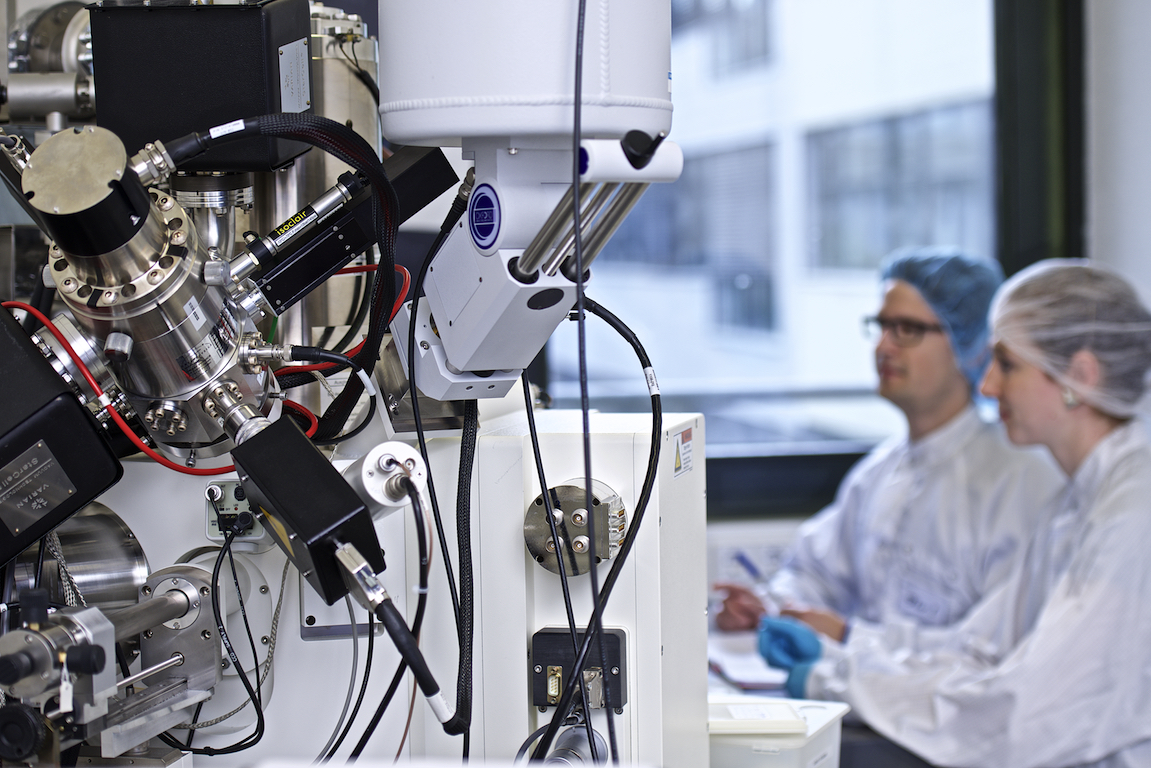
We employ two SEM-FIB systems, a Zeiss Neon 40 EsB and a Zeiss CrossBeam 1540XB, which are both equipped an ultra high resolution field emission (FE) SEM and a high performance FIB column.
The key features of both FESEMs are
- resolution: 1.1 nm @ 20 kV / 2.5 nm @ 1 kV
- acceleration voltage: 0.1-30 kV
- probe current: 4 pA-20 nA
The key features of both FIB columns are
- resolution: 7 nm @ 30 kV
- acceleration voltage: 3-30 kV
- probe current: 1 pA-50 nA
- multi channel gas injection system for material deposition and enhanced or selective etching
- high resolution live imaging during milling and polishing
The Zeiss Neon 40 EsB is intended for material analysis and TEM sample preparation, whereas the Zeiss CrossBeam 1540XB focuses on sample pattering via lithography.
overview of the individual configuration
Neon 40 EsB
material analysis system employing
- SE2 and InLens detector
- EDX detector
- EsB and 4QBSD detector
- EBSD detector
- TEM sample preparation
CrossBeam 1540XB
patterning system equippend with
- SE2 and InLens detector
- EDX detector
- 4QBSD detector
- STEM detector
- Elphy Plus lithography system
- fast beam blanker and two external pattern generators for lithography with e-beam and Ga+ - ion beam
short overview of SEM and FIB (german)
Danke! Diese Video wurde vom "Medienlabor AG Medienwissenschaft/Kamera und Schnitt: Lukas Burg" im Rahmen einer Webdokumentation zum 50jährigen Bestehen der Universität Konstanz erstellt.